How Semiconductor Equipment Makers Source High-Flatness Machined Parts
A wafer never complains when it is mishandled. It just becomes scrap two hundred process steps later, at the metrology station, where the root cause is impossible to trace. In semiconductor equipment, the machined parts that touch, carry, or enclose the wafer - end-effector arms, vacuum chucks, stage plates, chamber rings - carry tolerances and cleanliness requirements that would be absurd in almost any other industry. A 2-micron warp across a chuck face is the difference between a clean transfer and a particle event.
This guide is written the way an engineer would explain it to a colleague on the equipment side. We walk through why high flatness machining sets your yield ceiling, what ultra-clean machining actually demands, how vacuum chamber parts behave under vacuum, where PEEK machined parts beat metal, how to pick a CNC machining center that can hold the spec, and the mistakes we see equipment makers make most often when they go to source these parts. Every number here is a real process number, not a brochure.
We are Dongguan Licun Technology Co., Ltd., brand LusterControl - a Dongguan source factory focused on stainless steel mirror machining since 2015, now 15 years in. We run 60+ CNC machines on a 2,000 m2 floor at roughly 500,000 parts a month, holding ISO 9001, with ISO 13485 completed and IATF 16949 in application. We serve the semiconductor equipment supply chain alongside medical, automotive, and UAV programs, and we have shipped precision parts to brands such as De'Longhi, Donlim, and Breville.
Table of Contents
- 1. Why High Flatness Machining Decides Yield in Wafer Handling
- 2. What Ultra-Clean Machining Actually Requires in Semiconductor Components
- 3. Semiconductor Components That Fail Quietly (and Why)
- 4. Vacuum Chamber Parts: Flatness, Outgassing, and Leak Tightness
- 5. PEEK Machined Parts vs Metal in Semiconductor Tooling
- 6. Choosing the Right CNC Machining Center for Flatness-Critical Work
- 7. A Sourcing Checklist for High-Flatness Semiconductor Components
- 8. Common Sourcing Mistakes for Ultra-Clean Machining of Semiconductor Components
Semiconductor CNC precision component
Why High Flatness Machining Decides Yield in Wafer Handling
A 2-micron warp at the chuck is a wafer's worth of scrap.
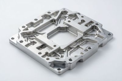
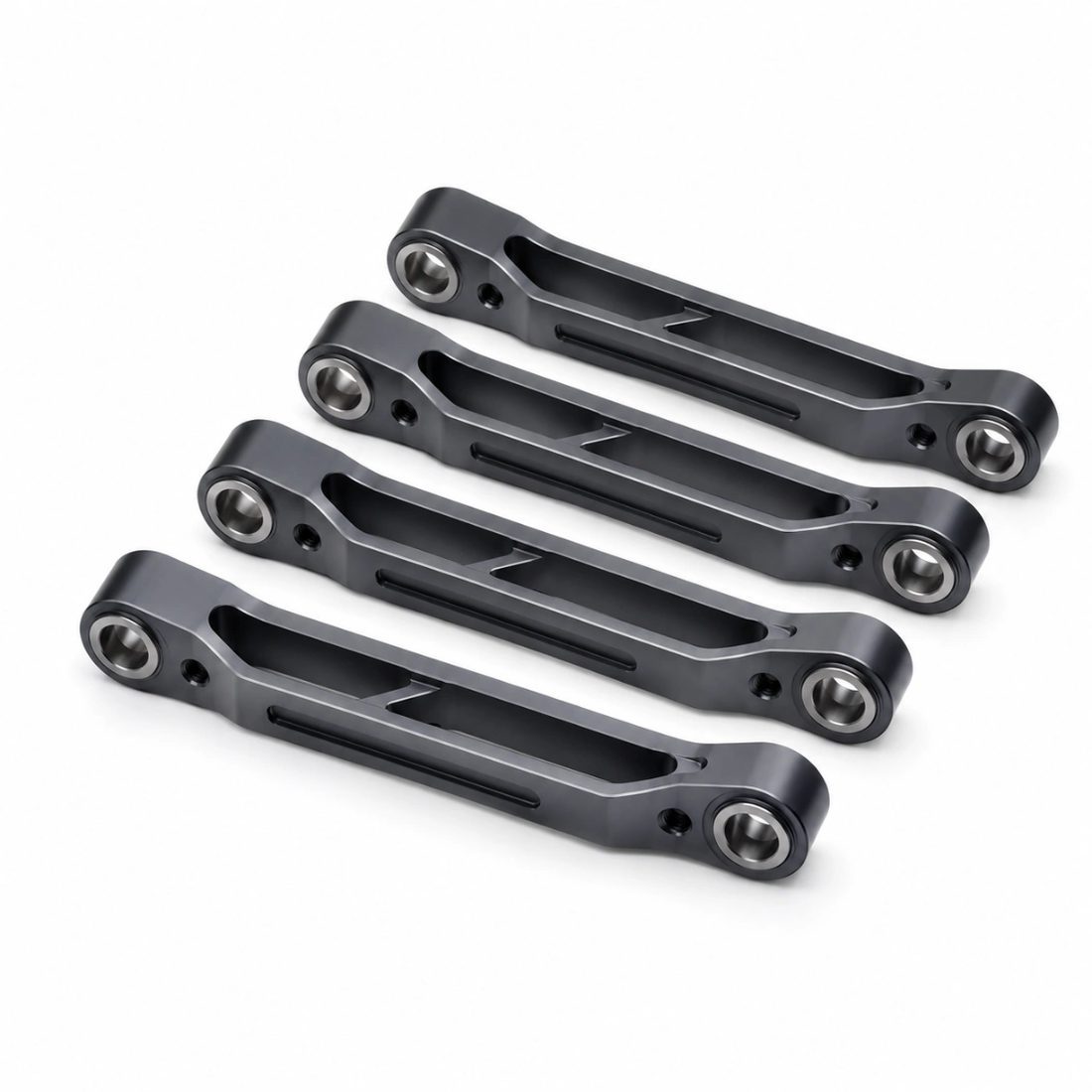
Wafer handling is unforgiving because the parts are both structural and clean. An end-effector that flexes by a few microns under vacuum load shifts the wafer's position; a vacuum chuck whose sealing face is not flat leaks and pulls particles; a stage plate that is not parallel to the optical axis throws off every alignment downstream. In this world, flatness and parallelism are not nice-to-haves - they are the yield ceiling.
High flatness machining is the discipline of holding a reference surface true to a datum within microns, then holding every feature that matters relative to that surface. We routinely hold flatness to 0.005 mm across a 200 mm plate and can lap or grind critical faces down toward 0.002 mm when the application needs it. The same single-datum discipline that keeps our standard precision at +/-0.005 mm positioning is what protects flatness through the whole operation.
How we hold flatness on stainless and aluminum
- Machine the part on one datum so the coordinate system never moves between faces.
- Stress-relieve or anneal before the finish pass so internal stress does not bow the part after machining.
- Finish by grinding or lapping the reference face to the final flatness, not by hoping the mill got it.
- Verify on a CMM with a full datum report - never trust a feeler gauge alone on a part this size.
| Part type | Typical flatness we hold | Why it matters |
|---|---|---|
| Vacuum chuck sealing face | 0.002 - 0.005 mm | Leak-tight seal, no particle pull |
| Wafer stage plate | 0.003 - 0.008 mm | Parallel to optical axis, stable alignment |
| End-effector arm | 0.01 mm | No drift under vacuum load |
| Guide rail bracket | 0.02 mm | Smooth travel, low vibration |
Semiconductor CNC precision component
What Ultra-Clean Machining Actually Requires in Semiconductor Components
Clean is a measurable spec, not a feeling.
In semiconductor components, contamination is measured in particles per square centimeter and ions per surface area. A fingerprint left on a chamber ring becomes an ionic contaminant that wrecks a gate oxide months later. Ultra-clean machining means the part leaves the building at a defined cleanliness level, with the process to prove it - not just a wipe before shipping.
Terms you will hear (and should ask about)
- ISO 14644
- The standard that defines cleanroom classes by particle count per volume of air - the reference for how clean your handling environment should be.
- Outgassing
- The release of trapped volatiles from a material into vacuum; high outgassing contaminates the chamber and lengthens pump-down.
- Ionic contamination
- Sodium, chloride and other ions left on a surface that can migrate and damage sensitive device layers.
- ASTM A967
- The standard for passivating stainless steel - rebuilds the chromium-oxide layer that resists corrosion and particle shedding.
Our cleaning and passivation flow
- Degrease to remove cutting fluid and handling oils completely.
- Passivate per ASTM A967 so the stainless surface resists corrosion and shedding.
- Rinse in deionized water to drop ionic residue.
- Bake out volatiles where the application is vacuum-rated.
- Package in clean, low-outgassing film immediately - not on a shop bench.
| Contamination type | Control method | Why it matters |
|---|---|---|
| Particles | Cleanroom handling + sealed pack | Cause defects at the wafer surface |
| Ions | DI rinse after passivation | Destroy thin gate oxides |
| Outgassing | Bake-out + low-outgassing material | Shortens pump-down, fouls vacuum |
| Burrs | Edge break + visual inspect | Burrs shed particles under load |
If you want to dig deeper into how we treat semiconductor components and the rest of our precision portfolio, our technical blog covers the process side in detail.
Semiconductor Components That Fail Quietly (and Why)
The expensive failures never make a sound.
Most semiconductor component failures are silent at first. A vacuum leak shows up as a longer pump-down time that nobody flags. A chuck that is 3 microns out of flat transfers wafers slightly off, and the yield dip is blamed on the process, not the part. By the time the root cause surfaces, a batch is lost. The job of good sourcing is to catch these modes before the part ships.
- Vacuum leaks from porous welds or unsealed threaded holes pull particles and extend pump-down.
- Particle shedding from rough internal surfaces or poor passivation contaminates the chamber.
- Thermal drift from mixed materials changes alignment as the tool heats to operating temperature.
- Burrs at edges that break off under motion and land on a wafer.
- Flatness loss after machining because residual stress was never relieved.
| Failure mode | Typical cause | How we catch it |
|---|---|---|
| Leak | Unsealed thread, porous weld | Helium-leak or pressure decay check |
| Particle event | Rough bore, no passivation | Profilometry + clean-pack audit |
| Misalignment | Flatness out of spec | CMM flatness report per lot |
| Drift | Mixed CTE materials | Design review before cutting |
The same quality discipline we apply to medical device components - documented traceability, first-article inspection, and lot-level verification - is what keeps these silent failures from ever reaching your line.
Semiconductor CNC precision component
Vacuum Chamber Parts: Flatness, Outgassing, and Leak Tightness
In vacuum, every surface is a gas source.
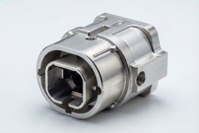
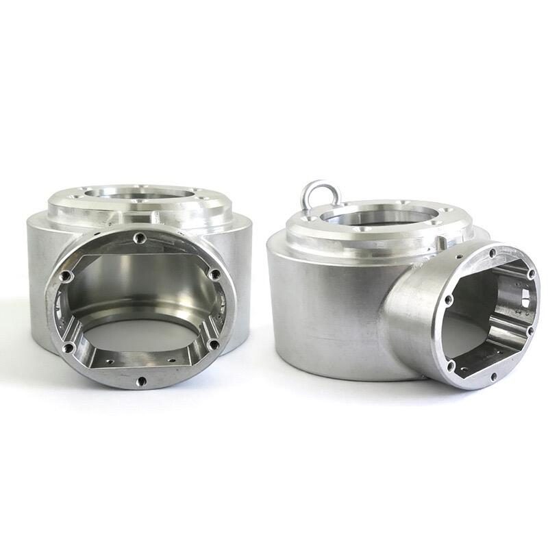
Vacuum chamber parts live in an environment where any impurity becomes a contaminant. The internal surfaces must be smooth enough not to trap gas, the seals must be flat enough to hold vacuum, and the material must be low-outgassing by nature or by treatment. A chamber ring made from the wrong alloy, or finished without passivation, quietly degrades the vacuum every cycle.
Materials and how they behave in vacuum
| Material | Outgassing | Best use in chamber |
|---|---|---|
| 6061 aluminum | Low after bake-out | Structural frames, plates |
| 304 / 316L stainless | Low, better after passivation | Chamber walls, rings, welds |
| PEEK | Very low | Insulators, pure-gas path parts |
| Brass / zinc alloys | High | Avoid in vacuum path |
Pros
- Stainless holds vacuum and resists corrosion
- Passivation drops outgassing and particle shedding
- Smooth internal finish shortens pump-down
- Low-outgassing plastics seal cleanly
Cons
- Stainless is heavier and pricier than aluminum
- Passivation adds a process step
- Tight flatness needs finish grinding
- Wrong alloy choice ruins the vacuum
We treat every vacuum-facing surface as a gas source: we specify the finish, passivate the stainless per ASTM A967, and verify the seal faces on a CMM so the part holds vacuum the first time it is bolted in.
PEEK Machined Parts vs Metal in Semiconductor Tooling
PEEK earns its place where metal fights back.
PEEK machined parts are not a downgrade from metal - they solve problems metal creates. PEEK is a high-purity engineering polymer with very low outgassing, excellent chemical resistance, and natural electrical insulation. In a gas-delivery path or an insulating spacer inside a chamber, PEEK keeps the process pure where a metal part would introduce ions or conductivity you do not want.
When PEEK wins the argument
- Electrical insulation is required and a coating on metal would flake.
- The part contacts high-purity or corrosive chemistry and must not react.
- Weight reduction matters and metal adds mass you cannot afford.
- Outgassing must be near zero and the material is inherently clean.
| Property | PEEK | 6061 aluminum | 316L stainless |
|---|---|---|---|
| Outgassing | Very low | Low after bake | Low after passivation |
| Electrical | Insulating | Conductive | Conductive |
| Chemical resist | Excellent | Good (anodized) | Excellent |
| Strength | Moderate | High | Very high |
| Use in chamber | Pure-gas, insulator | Structure | Walls, welds |
We machine PEEK on dedicated tooling so it does not pick up metal swarf, and we tumble or clean the parts in a low-particulate flow so the finished piece stays as pure as the material started.
Semiconductor CNC precision component
Choosing the Right CNC Machining Center for Flatness-Critical Work
The machine is only as honest as its thermal stability.
A CNC machining center that holds a tolerance at 8 a.m. but drifts by midday is useless for flatness-critical semiconductor work. Thermal stability, a rigid structure, and in-process probing matter more than the headline spec on the brochure. The question is not 'how many axes' but 'how consistently does it hold the datum across a shift.'
What to ask a supplier before you quote
- Do you machine on a single datum, or re-fixture between faces?
- What is your thermal compensation - climate-controlled cell, or hope?
- Do you probe in-process, or only inspect the finished part?
- Can you CMM every reference face, not just the tolerance-featured ones?
- Do you run 3+2 and 5-axis, or only 3-axis with re-clamps?
| Capability | What it gives you | Our floor |
|---|---|---|
| Single-datum 3+2 / 5-axis | No datum shift between faces | 60+ CNC, incl. 5-axis |
| In-process probing | Catch drift before scrap | Standard on precision cells |
| CMM first article | Prove the process before volume | Full datum report per FAI |
| Climate-controlled cells | Stable size across a shift | Controlled shop environment |
A Sourcing Checklist for High-Flatness Semiconductor Components
Hand this to a supplier and watch the weak ones bow out.
- Can they state a flatness target in microns and verify it with a CMM, not a feeler gauge?
- Do they passivate stainless per ASTM A967 and prove it with a finish report?
- Will they provide a first-article inspection with full datum references?
- Can they control outgassing and package in clean, low-outgassing film?
- Do they hold ISO 9001 at minimum, with ISO 13485 or IATF 16949 a plus?
- Is every lot traceable from raw bar to finished part, with material certs?
- Do they answer engineering questions with numbers, not sales talk?
- Can they scale from prototype to volume without re-qualifying the process?
A supplier that clears all eight is rare. One that stumbles on flatness verification or clean-pack should not be on a wafer-handling program. Send us your drawing for a free DFM review and we will tell you exactly which features drive the cost and which tolerances are worth holding tight.
Semiconductor CNC precision component
Common Sourcing Mistakes for Ultra-Clean Machining of Semiconductor Components
Most scrap was decided at the PO, not the machine.
- Specifying 'smooth' instead of an Ra number, then arguing about it after shipment.
- Skipping first-article inspection to save time - the cheapest insurance you have.
- Treating passivation as optional and wondering why the chamber corrodes.
- Mixing materials without designing for their different thermal expansion.
- Choosing a shop on price alone and discovering it cannot verify flatness.
- Ignoring traceability until a single complaint forces a full recall.
The cheapest machined part is the one that passes qualification the first time - because the second time costs you a launch date and a yield investigation.
Semiconductor CNC precision component
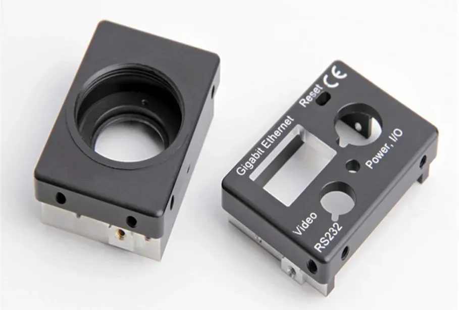
Semiconductor CNC precision component
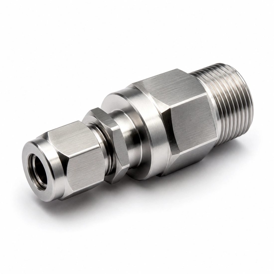
Semiconductor CNC precision component
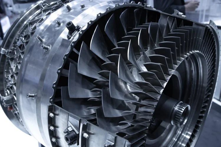
Semiconductor CNC precision component
FAQ: semiconductor components & Semiconductor Buyer Questions
A: For vacuum chuck sealing faces we routinely hold 0.002 to 0.005 mm, and stage plates around 0.003 to 0.008 mm. The right number depends on the reference surface and what it seats against; we CMM every reference face and report it, rather than guessing with a feeler gauge.
A: Yes, for insulators and pure-gas-path parts. PEEK has very low outgassing, excellent chemical resistance, and natural insulation, so it solves problems metal creates. Use metal for structure and seals, and design for the different thermal expansion if you mix them in one assembly.
A: We degrease, passivate stainless per ASTM A967, rinse in deionized water, bake out volatiles where the part is vacuum-rated, and package immediately in clean low-outgassing film. Internal surfaces are finished smooth and audited so they do not trap gas or shed particles.
A: Yes. Passivation per ASTM A967 rebuilds the chromium-oxide layer that resists corrosion and particle shedding - essential for any stainless part that lives in a vacuum or clean environment. We supply a finish report with the lot.
A: We hold ISO 9001, have completed ISO 13485, and are pursuing IATF 16949. The same documentation discipline - first-article inspection, in-process gauging, and lot-level traceability from raw bar to finished part - applies across our semiconductor, medical, and automotive programs.
A: Yes. Our Dongguan plant runs 60+ CNC machines and about 500,000 parts a month, so a program can grow from first article to full production while keeping the same documented process and traceability chain - no re-qualification of the source required.
Planning a wafer-handling or vacuum-chamber build and unsure which tolerances actually move the yield? Send us your drawing for a free DFM review - we will flag the features that need single-datum 5-axis work, the surfaces that must be passivated per ASTM A967, and the flatness numbers worth holding tight. No obligation, just a clear engineering answer.
Request a Free CNC Quote