Semiconductor Test Fixtures: Balancing ESD Protection and Flatness (2026 Guide)
If you build or buy test sockets, probe holders, or fixture plates for semiconductor final test, you already know the part that looks simplest on the drawing is often the one that decides your yield. A test socket does one job: hold the device under test flat and steady so every probe makes clean contact. Miss the flatness or let a static discharge sneak through, and you get false failures, cracked dies, and a test floor that quietly burns money on escapes and retries.
In this 2026 guide we walk through what semiconductor fixture machining actually demands, why flatness and ESD protection pull in opposite directions, and how material choice between 440C stainless and 7075 aluminum changes both. We cover the tolerance budget on probe holes and guide pins, where CNC precision machining beats manual work for lot-to-lot repeatability, and a sourcing checklist you can hand a supplier today. Everything here is written from a precision shop floor, not a catalog.
We have been a Dongguan source factory for precision CNC work since 2015, with 60 machines, a 4,000 sqm floor after our 2026 expansion, and monthly output around 500k parts. We machine semiconductor fixture and test socket parts in small custom batches and volume alike, and the trade-offs below are the ones we argue through with test engineers before the first article is cut.
Table of Contents
- 1. What Semiconductor Fixture Machining Demands From Your Shop
- 2. Test Socket Parts Machining: The Flatness Problem
- 3. Precision Machining for ESD-Safe Fixture Bodies
- 4. Tight Tolerance CNC Work on Probe Contacts and Guide Pins
- 5. CNC Precision Machining vs Manual Work for Test Sockets
- 6. Why Semiconductor Fixture and Test Socket Parts Need Material Traceability
- 7. A Buyer's Sourcing Checklist for Semiconductor Fixture Machining
- 8. Common Mistakes in Test Socket Parts Machining to Avoid
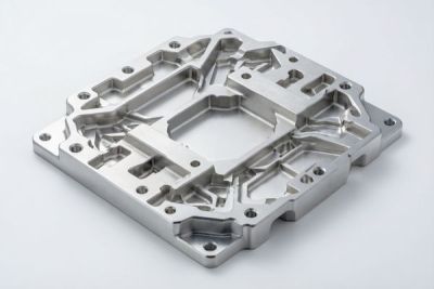
Semiconductor Assembly & Test / Wafer Fab Support CNC precision component
What Semiconductor Fixture Machining Demands From Your Shop
A fixture is a passive part doing an active job - holding microns still under contact force.
A test fixture or socket body looks like a plate with holes, but its function is unforgiving. The device under test rests on it, probes push down from above, and the whole stack has to stay geometrically true within a few microns while thousands of devices cycle through. That is why precision machining for these parts is less about hitting one number and more about holding a relationship - seat flatness to the probe plane, hole position to the package pitch, and surface behavior that neither insulates nor arcs.
The two enemies: flatness loss and static
Flatness loss shows up as open or marginal contacts; a 5-micron tilt across the seat can drop a corner of the package out of the probe's working window. Static shows up worse - a single discharge through a sensitive die can pass test and fail in the field weeks later. Good CNC precision machining tackles both at once: it controls the geometry, and it lets you choose a material and finish whose surface resistance sits in the safe ESD band.
- Test socket
- The replaceable interface that mates the package leads or balls to the tester's probe array during final test.
- Fixture plate / nest
- The base that locates and supports the device under test so every probe contacts consistently.
- Flatness
- The deviation of a seated surface from a perfect plane, measured in microns across the contact area.
- ESD-safe surface
- A finish whose surface resistance stays low enough to bleed static charge without shorting active circuitry.
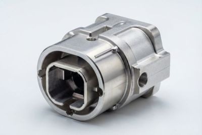
Semiconductor Assembly & Test / Wafer Fab Support CNC precision component
Test Socket Parts Machining: The Flatness Problem
Ask for 'flat' and you will get a number you did not define - so define it.
Flatness is the first thing a test engineer feels and the last thing a loose drawing specifies. On a socket seat, flatness governs how evenly the package presses into the probe array. Too much tilt and the corner probes never reach working compression, giving you intermittent opens that look like device failures, not fixture failures. The honest answer to 'how flat' is: flat enough for your pitch and probe height tolerance, and that number is different for a coarse-pitch power device than a fine-pitch logic part.
How flat is flat enough
We size the flatness callout to the probe's allowed compression window. A probe with 0.15 mm of usable travel can forgive more seat tilt than one with 0.05 mm. Below is the working table we use to start the conversation with customers; the right column is the seat flatness we target before the part leaves the shop.
| Device class | Pitch / probe travel | Seat flatness we target |
|---|---|---|
| Coarse power / leaded | 0.15 mm travel | 0.02 mm over seat |
| Standard QFN / BGA | 0.10 mm travel | 0.01 mm over seat |
| Fine-pitch logic | 0.05 mm travel | 0.005 mm over seat |
| Known-good-die contact | 0.03 mm travel | 0.003 mm over seat |
- Specify flatness over the actual contact area, not the whole blank
- Call out whether the number is measured clamped or free-state
- Match the probe travel window before tightening the flatness callout
- Inspect the first article on a granite or CMM plane, not a feeler gauge
Precision Machining for ESD-Safe Fixture Bodies
ESD protection is a material and finish decision long before it is a handling rule.
The two materials we most often machine for these parts tell the ESD story clearly. 440C stainless is hard, dimensionally stable, and naturally conductive, so a bare or lightly passivated surface sits in a safe static-dissipative band without extra coating. 7075 aluminum is lighter and cheaper to machine, but bare aluminum is a poor ESD story on its own; it needs a conductive (not insulative) anodize or a topcoat that keeps surface resistance in the dissipative range. The choice is rarely 'which is better' and almost always 'which fits the mass, stiffness, and handling budget of your handler'.
Conductive vs insulative surface resistance
Surface resistance is the number that decides whether static bleeds or builds. Insulative anodize can push a surface into the billions of ohms and turn your fixture into a capacitor; a conductive treatment keeps it in the 10 to the 9th ohm per square dissipative window where charge drains safely. We confirm the treatment class with you up front because it changes both the machining sequence and the final inspection.
| Material / finish | Surface resistance | Best fit |
|---|---|---|
| 440C stainless, bare / passivated | Dissipative (conductive) | Stable, repeatable seats, no coating |
| 7075 + conductive anodize | Dissipative window | Light handler parts, cost-driven |
| 7075 + standard insulative anodize | Insulative (high ohms) | Avoid for ESD-critical seats |
| Peek / filled polymer | Controlled dissipative | Non-marring, low-mass contact |
Pros
- 440C holds geometry through thermal cycles with no coating drift
- Conductive path is intrinsic, not a coating that wears off
- 7075 machines faster and lightens the handler
- Dissipative anodize keeps aluminum ESD-safe
Cons
- 440C is slower and harder on tooling than aluminum
- 7075 needs a specified conductive finish or it fails ESD
- Polymer seats wear and need replacement planning
- Wrong anodize class silently defeats the ESD intent
Semiconductor Assembly & Test / Wafer Fab Support CNC precision component
Tight Tolerance CNC Work on Probe Contacts and Guide Pins
The holes and pins are where the package either lands true or lands crooked.
Probe holes, guide pins, and locating bosses are the features that decide whether the device seats the same way every time. Their positional accuracy relative to each other matters more than any single dimension, because the whole alignment chain is only as good as its weakest true-position callout. This is where tight tolerance CNC earns its keep: single-setup machining keeps the datum fixed so hole-to-pin relationships stay true across the batch.
How we hold the tolerance budget
- Map which relationships are functional (hole-to-pin, seat-to-boss) and protect them first
- Machine all critical features in one setup so the datum never releases
- Leave 0.1 mm for a finishing pass on bores and seats
- Inspect the first article on a CMM with full datum references
- Gauge in-process and audit lots so drift shows before a bad batch ships
| Feature | Typical callout | How we hold it |
|---|---|---|
| Probe hole position | true pos +/-0.01 mm | Single-setup 5-axis / turn-mill |
| Guide pin diameter | h7 to pin | +/-0.005 mm finishing pass |
| Seat-to-boss relation | perpendicular 0.01 mm | One datum, no re-clamp |
| Boss height step | +/-0.02 mm | Z-axis touch-off per part |
CNC Precision Machining vs Manual Work for Test Sockets
Manual can cut one good part; CNC cuts a hundred that are all the same good part.
For a single prototype, a skilled hand can dial in a socket that works. The problem starts at lot two. Manual work drifts with operator, tool wear, and setup mood; the second dozen seats are rarely identical to the first. CNC precision machining bakes the process into a program and fixtures, so the fiftieth part matches the first within the tolerance band. For test sockets, where lot-to-lot consistency is the whole point, that repeatability is the reason most volume programs leave manual work behind after the first article passes.
Repeatability across a lot
We qualify a program on the first article, lock the process, then run in-process gauging so a drift in tool wear shows up as a gauge trend rather than a bad lot. That is the difference between 'we shipped good parts' and 'we can prove we shipped good parts' - and proof is what an audit or a yield investigation asks for.
| Dimension | Manual (per setup) | CNC (program + fixture) |
|---|---|---|
| Lot-to-lot repeatability | Operator-dependent | Program-locked, low drift |
| First-article to batch | Often differs | Matches within band |
| Scalability | Slow to scale | Prototype to 500k/month |
| Proof / traceability | Hard to document | CMM + lot records |

Semiconductor Assembly & Test / Wafer Fab Support CNC precision component
Why Semiconductor Fixture and Test Socket Parts Need Material Traceability
In semiconductor test, 'which heat of steel' is a real question, not paperwork.
When a fixture starts causing intermittent contacts months after install, the first question a yield engineer asks is about the material: which heat, which lot, what treatment. If the shop cannot answer, you are debugging blind. That is why semiconductor fixture and test socket parts should ship with material certs traceable to the heat lot and a lot record from raw bar to finished part. It turns a mystery into a lookup.
What to ask a supplier for
- Material cert traceable to the heat lot (440C per ASTM, 7075 per spec)
- Confirmation of the anodize or passivation class and its resistance band
- CMM first-article report with full datum references
- Lot-level traceability from raw bar to finished part
- A documented rework and containment path if a lot drifts
A Buyer's Sourcing Checklist for Semiconductor Fixture Machining
Hand this to a supplier and the tire-kickers sort themselves out.
Sourcing these parts is less about finding a cheap machine and more about finding a shop that understands test-floor intent. The questions below are the ones we are happy to answer with data, and they separate a real precision source from a broker with a logo. Tick the boxes before you release a purchase order, not after a bad lot reaches your handler.
- Confirm cert stack: ISO 9001 minimum, ISO 13485 a plus (in progress at our plant), IATF 16949 relevant for auto-grade
- Request material certs traceable to the heat lot, not just a mill sheet
- Agree the ESD finish class (conductive anodize vs bare 440C) before quoting
- Get a CMM first-article report, not a photo of a good part
- Define flatness over the real contact area and the measured condition
- Verify lot traceability and a real containment path for drift
The cheapest test socket is the one that passes qualification the first time, because the second time costs you a launch date and a yield investigation.
Semiconductor Assembly & Test / Wafer Fab Support CNC precision component
Common Mistakes in Test Socket Parts Machining to Avoid
Most socket failures are designed in the drawing, not made on the mill.
- Drawing flatness across the whole blank instead of the contact area, then fighting spring-back
- Specifying insulative anodize on aluminum and calling it ESD-safe
- Forgetting coating thickness when tolerancing a press-fit probe hole
- Mixing free-state and clamped measurements without saying which is which
- Treating the first manual prototype as proof the production lot will match
- Leaving probe-hole position as a 'nice to have' instead of a true-position callout
None of these are exotic failures. They are the routine ones we see on incoming drawings, and every one is cheaper to fix in the DFM review than on the test floor. That is the whole point of sending the drawing early: a half-hour design conversation beats a scrap lot and a slipped qualification.
Semiconductor Assembly & Test / Wafer Fab Support CNC precision component
Semiconductor Assembly & Test / Wafer Fab Support CNC precision component
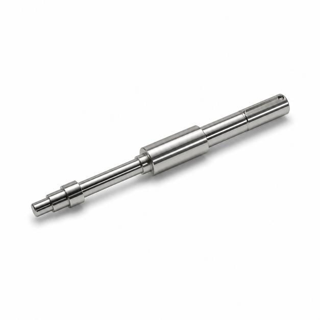
Semiconductor Assembly & Test / Wafer Fab Support CNC precision component
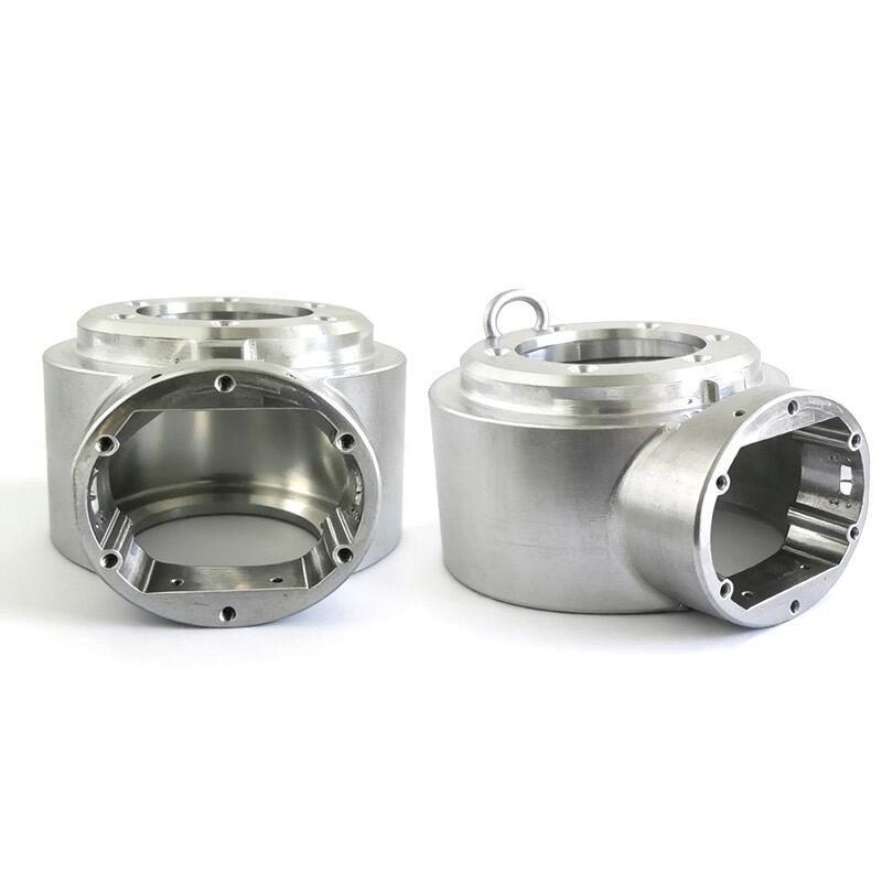
Semiconductor Assembly & Test / Wafer Fab Support CNC precision component
FAQ: semiconductor fixture and test socket parts & Semiconductor Assembly & Test / Wafer Fab Support Buyer Questions
A: It depends on your probe's usable travel. Coarse-pitch power devices with around 0.15 mm of probe travel can tolerate about 0.02 mm seat flatness, while fine-pitch logic near 0.05 mm travel needs closer to 0.005 mm. Always specify flatness over the real contact area and state whether it is measured clamped or free-state.
A: 440C is conductive on its own and dimensionally stable through thermal cycles, so it is the safe default for ESD-critical seats with no coating drift. 7075 machines faster and lightens the handler but needs a specified conductive anodize to stay in the dissipative resistance band; standard insulative anodize defeats the ESD intent. Choose on mass, stiffness, and handling budget.
A: Yes. We run single prototypes and small custom batches on the same 60-machine floor that supports volume, holding positional accuracy to +/-0.005 mm with single-setup machining so hole-to-pin relationships stay true. First articles get a full CMM report with datum references before the batch runs.
A: We confirm the surface-resistance class with you before quoting - bare or passivated 440C sits in a safe dissipative band intrinsically, while 7075 gets a specified conductive treatment. The number that matters is ohms per square in the 10 to the 9th range; we name it rather than loosely calling a part 'ESD-safe'.
A: Yes. We supply material certs traceable to the heat lot, a CMM first-article report, in-process gauging for batch parts, and lot-level traceability from raw bar to finished component. ISO 9001 certified, with our ISO 13485 system established and certification in progress and IATF 16949 in application.
A: Single prototypes are routine, and our floor is built for both small custom batches and volume up to around 500k parts a month across 60 machines. For a dedicated socket program we typically qualify at low volume, lock the CMM-verified process, then scale once the data is stable.
Send us your test socket or fixture drawing for a free DFM review - we will flag the flatness callout that needs tightening, the ESD finish that should change, and the probe-hole tolerances that are costing you yield. Reach out and let's cut the first article.
Request a Free CNC Quote