Semiconductor Fixture and Test Socket Parts: ESD vs Flatness Guide (2026)
If you buy or design semiconductor test fixtures, the two numbers that quietly decide your first-pass yield are flatness and ESD safety. The socket presses a bare die or packaged part against dozens of spring probes thousands of times a day, so a few microns of warp or one static-unsafe surface can flip a good device to a failure on the tester. Most spec sheets treat these as separate footnotes — but in the real fixture they fight each other.
This is a buyer's and engineer's view, not a shop-floor brag. We walk through what semiconductor fixture and test socket parts actually have to survive, why ESD protection and flatness pull in opposite directions, and how to choose the material and machining route that holds both — without over-paying for tolerance you cannot use or under-buying the flatness your contact plan demands.
LusterControl (Dongguan Licun Technology Co., Ltd.) is a Dongguan, China source factory with 15 years in precision CNC machining, 60 CNC machines and a 4,000 m2 plant. We run turning, 5-axis milling, grinding and mirror finishing in-house, so the trade-offs below are what we see on the CMM readout and the ESD audit, not a textbook ideal.
Table of Contents
- 1. What Semiconductor Fixture and Test Socket Parts Actually Must Survive
- 2. ESD and Flatness in Semiconductor Fixture Machining
- 3. Test Socket Parts Machining: Holding Flatness to Microns
- 4. CNC Precision Machining Paths to Burr-Free Edges
- 5. Tight Tolerance CNC for Probe-Socket Alignment
- 6. Precision Machining Material Choices: 440C Stainless vs 7075 Aluminum
- 7. Semiconductor Fixture and Test Socket Parts Buyer's Checklist
- 8. Common Mistakes in Test Socket Parts Machining
- 9. CNC Precision Machining Roadmap: Send Us Your Drawing for DFM
Semiconductor Assembly & Test / Wafer Fab Support CNC precision component
What Semiconductor Fixture and Test Socket Parts Actually Must Survive
Before any flatness number matters, you have to know what the socket is really up against.
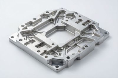
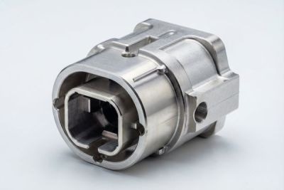
Semiconductor fixture and test socket parts sit at the boundary between the device under test and the tester. A test socket holds the package while spring probes make contact; a probe-socket carrier aligns the whole array. Every cycle repeats the same stresses: mechanical z-axis force, thermal swing from the handler, and — the part people forget — electrostatic discharge risk from handling and from the device itself. The fixture has to be flat enough that every probe seats, stiff enough that it does not creep, and ESD-safe enough that it does not zap the part it is meant to validate.
- Test socket
- A precision carrier that holds a packaged semiconductor device in place and presents its leads/pads to spring probes on the tester. Flatness of the seating plane is what keeps all contacts in spec.
- ESD (electrostatic discharge)
- A sudden current between two objects at different potentials. In a test fixture it can damage sensitive dies, so surfaces and handling must be controlled to dissipate or block charge safely.
- Flatness
- The deviation of a surface from a perfect plane, usually stated in microns. For probe seating it sets how evenly each contact is loaded across the array.
The practical question for a buyer is not 'how flat can they go' but 'which flatness and which ESD strategy does my contact plan actually need, with a record I can audit.' A burn-in socket that runs hot for hours has a different driver than a final-test socket that must be burr-free for a clean probe strike. Confusing the two is the most expensive mistake in this category.
Semiconductor Assembly & Test / Wafer Fab Support CNC precision component
ESD and Flatness in Semiconductor Fixture Machining
The core tension: the material that wins on flatness often fights you on ESD, and vice versa.
Semiconductor fixture machining has to balance two physical goals. Flatness wants a hard, dimensionally stable material that does not relax under clamp load or thermal cycling. ESD safety wants a surface that either conducts charge away (conductive) or blocks it (dissipative/insulating, controlled). The conflict is concrete: hardenable 440C stainless is stable and holds flatness beautifully, but as a bare metal it is also conductive — which is fine for dissipation but demands careful isolation design. 7075 aluminum is lighter and easier to hold flat in volume, but a standard anodize layer turns it into an insulator that can trap charge unless you specify an ESD-safe finish.
| Driver | What it wants | What it costs you if ignored |
|---|---|---|
| Flatness | Hard, stable, low-creep material | Probe mis-seating, contact resistance drift |
| ESD safety | Controlled conductive or dissipative surface | Latent device damage, field returns |
| Repeatability | Tight, documented tolerance | Yield loss that looks like a 'device' problem |
| Throughput | Low-friction, burr-free contacts | Worn probes, re-test loops |
The engineering move is to stop treating ESD as a coating you add at the end and start treating it as a material-and-route decision made at the RFQ. Decide early whether the socket body should dissipate charge (conductive path to ground plane) or block it (controlled insulating barrier with safe handling), then pick the machining route that still holds the flatness your contact plan needs.
Test Socket Parts Machining: Holding Flatness to Microns
How the route you pick changes the flatness you can actually hold and audit.
Test socket parts machining reaches micron flatness two ways: a precision grinding or fine finishing pass on the CNC cell, or machining followed by in-house flat-lapping so the part never leaves the building. Keeping it in one plant is the difference between a single quality record and a broken one. The table below shows what each route realistically delivers in our Dongguan facility across 60 CNC machines.
| Process | As-machined flatness | Best flatness at LusterControl | Best for |
|---|---|---|---|
| CNC turning (Swiss-type) | Ra 0.8-1.6 um, +/-0.01 mm | Flat seat to +/-0.005 mm | Rotational inserts, pins, spacers |
| 3-5 axis CNC milling | Ra 0.8-3.2 um, +/-0.01 mm | Flat seat to +/-0.005 mm | Socket frames, non-round carriers |
| Precision grinding | Ra 0.2-0.8 um, +/-0.005 mm | Flatness to single-digit microns | Seating planes, reference flats |
| Flat-lap + polish | n/a (finish step) | 8K mirror Ra 0.2 um on seat | Optical/clean contact faces |
Two things jump out. First, grinding already lands near your flatness target without a separate lap step, which is why it dominates seating-plane work. Second, a true mirror Ra 0.2 um seat only appears after flat-lapping or polishing — no cutting process gets you there alone. For most test sockets the smart move is a fine milling or grinding pass for geometry, then a light in-house lap only on the contact face, so 60 machines and 4,000 m2 of capacity run as one auditable line.
Semiconductor Assembly & Test / Wafer Fab Support CNC precision component
CNC Precision Machining Paths to Burr-Free Edges
A burr you cannot see is the fastest way to break a clean probe strike.
CNC precision machining for test sockets is as much about what is NOT there — burrs, edges, chips trapped in a blind hole — as what is. A single raised edge on a probe guide can cock a spring pin and shift its contact point by tens of microns, which reads on the tester as a device failure. The reliable route at LusterControl is machining plus in-house deburring and electropolishing so the part keeps one lot-traceable quality record instead of being shipped to a second shop for finish.
| Factor | In-house CNC + polish (LusterControl) | Outsourced manual finish |
|---|---|---|
| Lead time | Single PO, ~7-day first article | +5 to 10 days on a handoff |
| Traceability | Lot-to-machine, one record | Chain breaks at the subcontractor |
| Edge consistency | SPC / CPK controlled | Operator-dependent |
| ESD control | One controlled process window | Hard to audit across shops |
Pros
- Choose in-house CNC + deburr + electropolish if you need burr-free edges and a single auditable ESD-safe record on a recurring socket program.
- Choose a hardenable 440C route if dimensional stability under thousands of cycles is the dominant driver.
Cons
- Avoid outsourcing the finish if your program requires lot traceability back to the cutting machine — the handoff usually severs it.
- Avoid electropolishing a purely structural frame where Ra 0.8 um would have passed and only added cost.
For most socket programs the right model is a finishing pass on the CNC cell, then a light in-house polish only on the contact face. See how our plant is laid out for single-record production.
Tight Tolerance CNC for Probe-Socket Alignment
Size and position are what make every probe strike the same place, every time.
Tight tolerance CNC and flatness are partners here, not rivals. The socket frame must hold the device pocket within a tight position tolerance so each spring probe lands on its pad, and the seating plane must stay flat so the contact force is even. Aggressive removal to hit a pocket tolerance can leave a rough seat; polishing to hit flatness can remove just enough stock to shift a critical dimension. The discipline is to hold +/-0.005 mm first, then plan the finish allowance so lapping lands you inside both specs at once.
The buyer takeaway: ask for the finish allowance on the drawing, not just the two numbers. A supplier who plans the lap stock is protecting your position tolerance; one who polishes 'until it looks right' is gambling with your alignment. LusterControl issues first-article CMM data on every new print so you can see pocket position, flatness and Ra on the same report.

Semiconductor Assembly & Test / Wafer Fab Support CNC precision component
Precision Machining Material Choices: 440C Stainless vs 7075 Aluminum
The material table that decides both flatness stability and ESD behavior.
Precision machining for semiconductor fixtures usually comes down to two workhorses: hardened 440C stainless and 7075 aluminum. Both machine cleanly in our shop; they just serve different masters. 440C takes and holds a hard, stable seat and resists the creep that wrecks flatness over thousands of cycles, but it is conductive and must be designed into an ESD-safe isolation or dissipation scheme. 7075 is lighter, faster to mill in volume and easy to hold flat, but a standard anodize makes it an insulator — so you must spec an ESD-safe finish if charge control matters.
| Property | 440C stainless (hardened) | 7075 aluminum |
|---|---|---|
| Dimensional stability | Excellent, low creep | Good, lightens handler load |
| Flatness hold | Best under thermal cycling | Very good, easier to lap |
| ESD behavior | Conductive — needs isolation design | Anodize = insulator; spec ESD-safe finish |
| Machinability / speed | Slower, harder tooling | Fast, high volume |
| Weight | Heavier | Lighter (handler friendlier) |
| Best use | Stable seats, long-life sockets | High-volume frames, light carriers |
| If your socket needs... | Recommended material + route | Why it wins |
|---|---|---|
| Long-life burn-in, stable seat | 440C + grinding + in-house lap | Holds flatness through thermal cycles |
| High-volume final test, light | 7075 + ESD-safe anodize + mill | Fast, light, charge-controlled |
| Burr-free clean contact | Either + electropolish | Mirror Ra 0.2 um, no edge transfer |
| Tight pocket position | Either + tight tolerance CNC | +/-0.005 mm, single record |
For most programs the deciding factor is lifecycle, not unit price: a 440C seat that survives ten times the cycles may beat a cheaper aluminum frame that creeps out of flatness. See our related technical guide on mirror-finish walls for vacuum chambers.
Semiconductor Fixture and Test Socket Parts Buyer's Checklist
Five things to demand in writing before you release a drawing.
Test socket quotes vary wildly because suppliers quietly assume different things about flatness datum, ESD strategy and finish route. Lock these five down in the RFQ and you remove most of the risk before the first chip is cut.
- Flatness value AND reference datum in writing (e.g. seat flat to 0.01 mm over the pocket plane).
- ESD strategy stated: conductive dissipation vs controlled insulating barrier — plus the finish spec.
- Pocket position tolerance and finish allowance on the drawing, not just the two end numbers.
- First-article CMM + material cert (ASTM A967 covers stainless passivation — confirm applicable).
- NDA and controlled CAD access if the socket is proprietary to your device.
If a supplier cannot tick all five, the cheap quote is the expensive one. Send us your drawing for a free DFM review and we return achievable flatness, tolerance, ESD route and a unit-price curve before you commit.
Semiconductor Assembly & Test / Wafer Fab Support CNC precision component
Common Mistakes in Test Socket Parts Machining
The errors that turn a flatness spec into a yield problem.
- Over-specifying flatness 'just to be safe' — pay for the function, not the micron you will never use.
- Forgetting the reference datum, then arguing about a number measured from the wrong plane.
- Outsourcing finish and losing lot traceability needed for automotive / medical-grade audit.
- No finish allowance on the print, so lapping drifts the critical pocket position.
- Choosing the wrong material (e.g. anodized aluminum where a stable 440C seat was the real need).
Every one of these is avoidable at the RFQ stage. A 15-minute DFM call saves the rework, the scrap and the finger-pointing later. That is exactly the conversation we have with De'Longhi, Donlim and Breville-grade programs before any steel or aluminum is cut.
CNC Precision Machining Roadmap: Send Us Your Drawing for DFM
From a flatness and ESD callout on paper to a socket you can audit.
For your semiconductor fixture the same model applies: turning, 5-axis milling, grinding, mirror and electropolishing all in-house, one quality record, one accountable partner in Dongguan. Read more process breakdowns on our blog or start with a drawing.
Semiconductor Assembly & Test / Wafer Fab Support CNC precision component
Semiconductor Assembly & Test / Wafer Fab Support CNC precision component
Semiconductor Assembly & Test / Wafer Fab Support CNC precision component
Semiconductor Assembly & Test / Wafer Fab Support CNC precision component
FAQ: semiconductor fixture and test socket parts & Semiconductor Assembly & Test / Wafer Fab Support Buyer Questions
A: Most seating planes target flatness in the single-digit-to-ten micron range with a stated reference datum; LusterControl holds a documented +/-0.005 mm tolerance and can lap seats to single-digit microns on 60 CNC machines. The right number depends on your probe plan, not a generic 'as flat as possible'.
A: It can be, but a standard anodize turns 7075 into an insulator that traps charge. You must specify an ESD-safe finish or design a conductive dissipation path. 440C stainless is conductive by nature and needs an isolation or dissipation scheme instead. The choice is a material-and-route decision made at the RFQ, not a coating added later.
A: Yes. Hold +/-0.005 mm position first, then plan the finish allowance so lapping lands you inside both the pocket position and the flatness spec at once. LusterControl issues first-article CMM data showing pocket position, flatness and Ra on one report.
A: A single plant keeps one lot-traceable quality record and one controlled ESD process window. Outsourcing the polish or lap usually severs traceability back to the cutting machine and makes the ESD audit harder — a real problem for automotive or medical-grade programs.
A: Yes. Every batch ships with lot-level traceability back to material and machine, plus first-article CMM data. We are ISO 9001 certified, run an ISO 13485 quality system (certification advancing) and apply IATF 16949 controls.
Want the right material and machining route on your next semiconductor fixture? Send LusterControl your drawing and our engineering team will return a free DFM review with the achievable flatness, ESD strategy, tolerance plan and a unit-price curve.
Request a Free CNC Quote